- 您现在的位置:买卖IC网 > Sheet目录2006 > LTC2621IDD-1#PBF (Linear Technology)IC DAC 12BIT R-R 10-DFN
LTC2601/LTC2611/LTC2621
4
2601fb
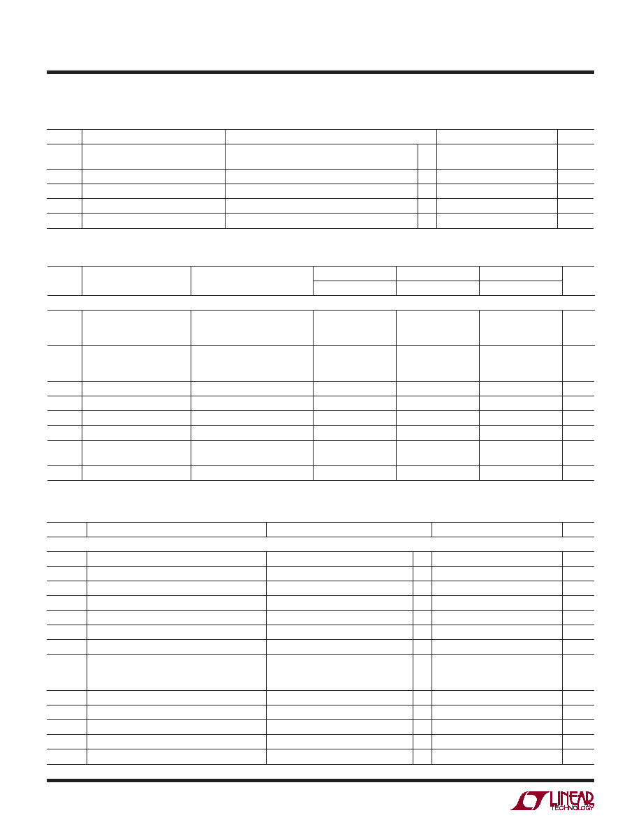
SYMBOL PARAMETER
CONDITIONS
MIN
TYP
MAX
UNITS
VIL
Digital Input Low Voltage
VCC = 4.5V to 5.5V
VCC = 2.5V to 5.5V
l
0.8
0.6
V
VOH
Digital Output High Voltage
Load Current = –100μA
l VCC – 0.4
V
VOL
Digital Output Low Voltage
Load Current = +100μA
l
0.4
V
ILK
Digital Input Leakage
VIN = GND to VCC
l
±1
μA
CIN
Digital Input Capacitance
(Note 4)
l
8pF
ELECTRICAL CHARACTERISTICS The l denotes the specications which apply over the full operating
temperature range, otherwise specications are at TA = 25°C. REF = 4.096V (VCC = 5V), REF = 2.048V (VCC = 2.5V), VOUT unloaded,
unless otherwise noted. (Note 8)
The
l denotes the specications which apply over the full operating temperature range, otherwise specications are at TA = 25°C.
REF = 4.096V (VCC = 5V), REF = 2.048V (VCC = 2.5V), VOUT unloaded, unless otherwise noted.
SYMBOL PARAMETER
CONDITIONS
LTC2621/ LTC2621-1
LTC2611/ LTC2611-1
LTC2601/ LTC2601-1
UNITS
MIN
TYP
MAX
MIN
TYP
MAX
MIN
TYP
MAX
AC Performance
tS
Settling Time (Note 6)
±0.024% (±1LSB at 12 Bits)
±0.006% (±1LSB at 14 Bits)
±0.0015% (±1LSB at 16 Bits)
77
9
7
9
10
μs
Settling Time for 1LSB Step
(Note 7)
±0.024% (±1LSB at 12 Bits)
±0.006% (±1LSB at 14 Bits)
±0.0015% (±1LSB at 16 Bits)
2.7
4.8
2.7
4.8
5.2
μs
Voltage Output Slew Rate
0.80
V/μs
Capacitive Load Driving
1000
pF
Glitch Impulse
At Midscale Transition
12
nV s
Multiplying Bandwidth
180
kHz
en
Output Voltage Noise
Density
At f = 1kHz
At f = 10kHz
120
100
120
100
120
100
nV/√Hz
Output Voltage Noise
0.1Hz to 10Hz
15
μVP-P
TIMING CHARACTERISTICS The l denotes the specications which apply over the full operating temperature
range, otherwise specications are at TA = 25°C. (See Figure 1) (Notes 4, 8)
SYMBOL
PARAMETER
CONDITIONS
MIN
TYP
MAX
UNITS
VCC = 2.5V to 5.5V
t1
SDI Valid to SCK Setup
l
4ns
t2
SDI Valid to SCK Hold
l
4ns
t3
SCK High Time
l
9ns
t4
SCK Low Time
l
9ns
t5
CS/LD Pulse Width
l
10
ns
t6
LSB SCK High to CS/LD High
l
7ns
t7
CS/LD Low to SCK High
l
7ns
t8
SDO Propagation Delay from SCK Falling Edge
CLOAD = 10pF
VCC = 4.5V to 5.5V
VCC = 2.5V to 5.5V
l
20
45
ns
t9
CLR Pulse Width
l
20
ns
t10
CS/LD High to SCK Positive Edge
l
7ns
t12
LDAC Pulse Width
l
15
ns
t13
CS/LD High to LDAC High or Low Transition
l
200
ns
SCK Frequency
50% Duty Cycle
l
50
MHz
发布紧急采购,3分钟左右您将得到回复。
相关PDF资料
LTC2630HSC6-LZ12#TRPBF
IC DAC 12BIT R-R SC70-6
LTC2642IDD-16#PBF
IC DAC 16BIT VOUT 10-DFN
LTC2704IGW-16#PBF
IC DAC 16BIT QUAD VOUT 44-SSOP
LTC2751AIUHF-16#PBF
IC DAC 16BIT CUR OUT 38-QFN
LTC2752ACLX#PBF
IC DAC 16BIT DUAL CUR OUT 48LQFP
LTC2753AIUK-16#TRPBF
IC DAC 16BIT DUAL 48-QFN
LTC2754AIUKG-16#PBF
IC DAC 16BIT QUAD IOUT 52-QFN
LTC2755AIUP-16#PBF
IC DAC 16BIT CUR OUT 64-QFN
相关代理商/技术参数
LTC2621IDD-1#TRPBF
功能描述:IC DAC 12BIT SGL R-R VOUT 10DFN RoHS:是 类别:集成电路 (IC) >> 数据采集 - 数模转换器 系列:- 产品培训模块:Data Converter Fundamentals
DAC Architectures 设计资源:Unipolar, Precision DC Digital-to-Analog Conversion using AD5450/1/2/3 8-14-Bit DACs (CN0052)
Precision, Bipolar, Configuration for AD5450/1/2/3 8-14bit Multiplying DACs (CN0053)
AC Signal Processing Using AD5450/1/2/3 Current Output DACs (CN0054)
Programmable Gain Element Using AD5450/1/2/3 Current Output DAC Family (CN0055)
Single Supply Low Noise LED Current Source Driver Using a Current Output DAC in the Reverse Mode (CN0139) 标准包装:10,000 系列:- 设置时间:- 位数:12 数据接口:DSP,MICROWIRE?,QSPI?,串行,SPI? 转换器数目:1 电压电源:单电源 功率耗散(最大):- 工作温度:-40°C ~ 125°C 安装类型:表面贴装 封装/外壳:SOT-23-8 薄型,TSOT-23-8 供应商设备封装:TSOT-23-8 包装:带卷 (TR) 输出数目和类型:1 电流,单极;1 电流,双极 采样率(每秒):2.7M
LTC-2621JD
功能描述:LED 显示器和配件 3 Digit, Red Low Current RoHS:否 制造商:Avago Technologies 显示器类型:7 Segment 数位数量:2 字符大小:7.8 mm x 14.22 mm 照明颜色:Red 波长:628 nm 共用管脚:Common Anode 工作电压:2.05 V 工作电流:20 mA 最大工作温度:+ 85 C 最小工作温度:- 35 C 封装:Tube
LTC-2621JD-01
制造商:Lite-On Semiconductor Corporation 功能描述:DISPLAY,CLOCK,3-DIG,ALINGAP RED,LOW-CUR,0.28",CAMPX - Rail/Tube
LTC-2621P
功能描述:LED 显示器和配件 3 Digit, Red RoHS:否 制造商:Avago Technologies 显示器类型:7 Segment 数位数量:2 字符大小:7.8 mm x 14.22 mm 照明颜色:Red 波长:628 nm 共用管脚:Common Anode 工作电压:2.05 V 工作电流:20 mA 最大工作温度:+ 85 C 最小工作温度:- 35 C 封装:Tube
LTC-2621WC
功能描述:LED 显示器和配件 3 Digit, Red Low Current RoHS:否 制造商:Avago Technologies 显示器类型:7 Segment 数位数量:2 字符大小:7.8 mm x 14.22 mm 照明颜色:Red 波长:628 nm 共用管脚:Common Anode 工作电压:2.05 V 工作电流:20 mA 最大工作温度:+ 85 C 最小工作温度:- 35 C 封装:Tube
LTC-2621Y
功能描述:LED 显示器和配件 3 Digit, Yellow RoHS:否 制造商:Avago Technologies 显示器类型:7 Segment 数位数量:2 字符大小:7.8 mm x 14.22 mm 照明颜色:Red 波长:628 nm 共用管脚:Common Anode 工作电压:2.05 V 工作电流:20 mA 最大工作温度:+ 85 C 最小工作温度:- 35 C 封装:Tube
LTC2622CMS8
功能描述:IC DAC 12BIT DUAL R-R VOUT 8MSOP RoHS:否 类别:集成电路 (IC) >> 数据采集 - 数模转换器 系列:- 产品培训模块:LTC263x 12-, 10-, and 8-Bit VOUT DAC Family 特色产品:LTC2636 - Octal 12-/10-/8-Bit SPI VOUT DACs with 10ppm/°C Reference 标准包装:91 系列:- 设置时间:4µs 位数:10 数据接口:MICROWIRE?,串行,SPI? 转换器数目:8 电压电源:单电源 功率耗散(最大):2.7mW 工作温度:-40°C ~ 85°C 安装类型:表面贴装 封装/外壳:14-WFDFN 裸露焊盘 供应商设备封装:14-DFN-EP(4x3) 包装:管件 输出数目和类型:8 电压,单极 采样率(每秒):*
LTC2622CMS8#PBF
功能描述:IC DAC 12BIT DUAL R-R VOUT 8MSOP RoHS:是 类别:集成电路 (IC) >> 数据采集 - 数模转换器 系列:- 产品培训模块:Lead (SnPb) Finish for COTS
Obsolescence Mitigation Program 标准包装:50 系列:- 设置时间:4µs 位数:12 数据接口:串行 转换器数目:2 电压电源:单电源 功率耗散(最大):- 工作温度:-40°C ~ 85°C 安装类型:表面贴装 封装/外壳:8-TSSOP,8-MSOP(0.118",3.00mm 宽) 供应商设备封装:8-uMAX 包装:管件 输出数目和类型:2 电压,单极 采样率(每秒):* 产品目录页面:1398 (CN2011-ZH PDF)